Sputtering Equipment EC7800
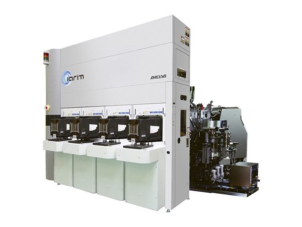
EC7800 is sputtering equipment designed for multi-layer deposition processes, integrating the proven technologies of the HC7100 series for magnetic devices and the IC7000 series for semiconductor devices.
Information
- Multi-layer deposition processes (MRAM, Magnetic sensor, etc.)
- Memory devices such as non-volatile memory
- Atomic-level thickness uniformity and precise film thickness control
- Achieving high-quality interface control by integrating processing modules such as etching and heating
- Multi-layer deposition under ultrahigh-vacuum
- Substrate size : Φ8-inch, Φ12-inch
- Number of installed modules : up to 10 modules
- Configurable modules : etching, oxidation, heating, cooling