We have launched our new product "Adastra" series
Oct. 9, 2024
CANON ANELVA CORPORATION
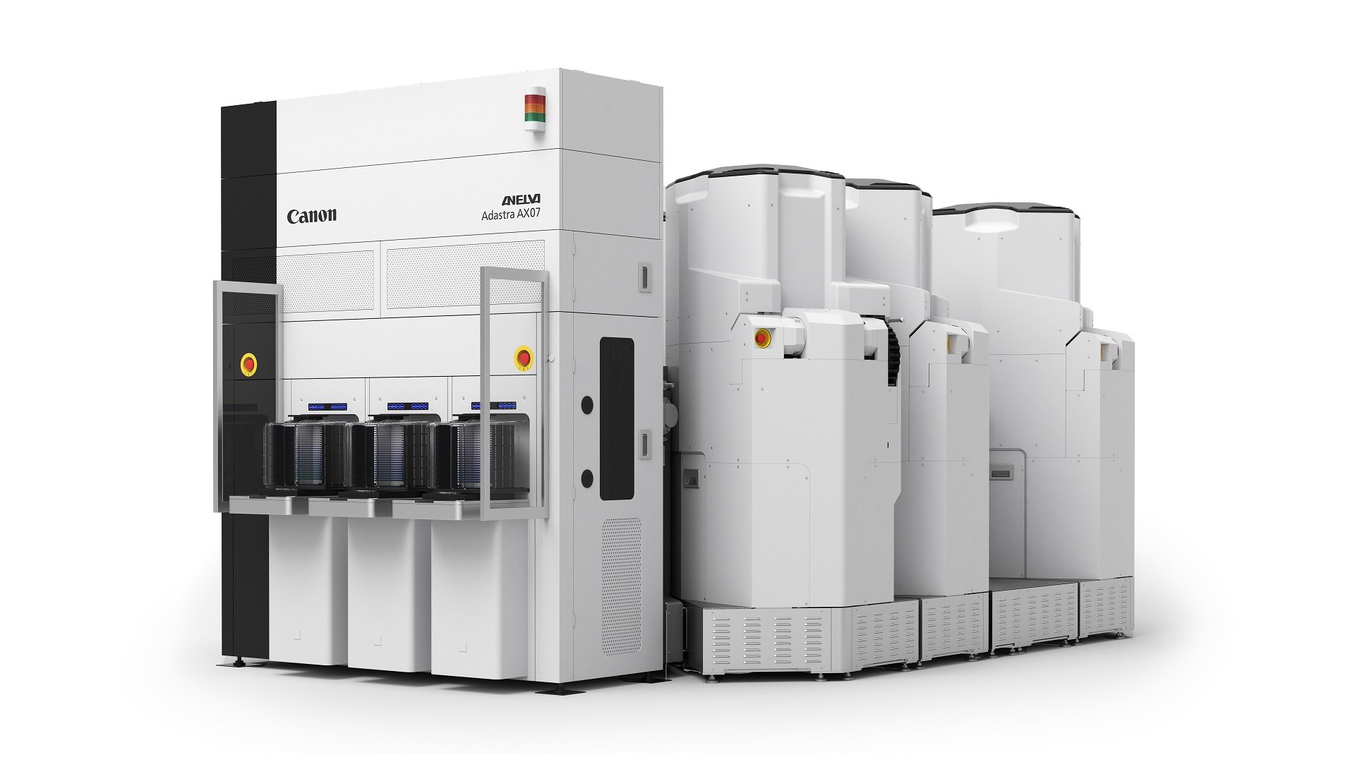
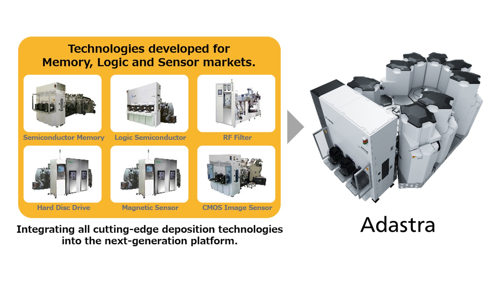
CANON ANELVA Corporation has launched a new “Adastra” product family for the manufacturing of semiconductor and electronic devices. It flexibly integrates a wide range of sputtering technologies developed over many years. This platform allows for a quick response to the diverse and complex needs of the market and its users.
The new “Adastra” product family has been released, encompassing a wide range of deposition processes, including those for interconnects and functional layers in semiconductor and electronic devices.

The deposition technologies developed over the years for various devices are integrated into the Adastra platform, based on a unified design concept. Adastra flexibly meets diverse needs by allowing users to freely select process modules from its lineup. Additionally, Adastra has significantly reduced its footprint and energy consumption compared to current products, thereby offering added value.

■ Integration of Film Deposition Technologies and Flexible Equipment Configuration
With diversification of semiconductor and electronic devices, manufacturing processes are becoming increasingly complex. Adastra can build a system that meets these requirements, allowing users to freely select the necessary process modules based on their demands. Additionally, its flexible equipment configuration supports a wide range of activities, from R&D to mass production, enabling seamless process transfer.
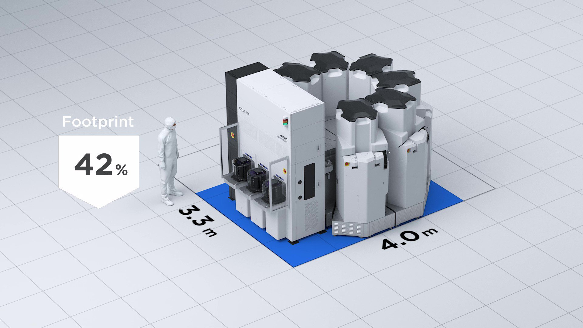
■ Space Saving Design
Adastra achieves a significant 42% reduction in footprint by miniaturizing the modules compared to current equipment. Similar space saving is also realized in the sub-fab area by reducing the number of electrical racks and pumps.

■ Usability
Workability during maintenance tasks, such as shield replacement, is improved through ergonomic design. Automated equipment start-up after maintenance enables immediate mass production. Real-time monitoring of equipment and displayed module information support predictive maintenance planning.
■ Eco-friendly
The miniaturization of the equipment reduces raw material usage by 7% and transportation energy by 8%, thanks to weight reduction. Additionally, cooling water consumption is decreased by 55% through the use of a circulated system instead of facility water. These improvements collectively reduce CO2 emissions by 18%. Adastra minimizes environmental impact and represents a step forward in realizing an environmentally friendly future.
Canon ANELVA contributes to the growth of the semiconductor and electronic devices industries.