Deposition (sputtering)
What is Thin Film Deposition?
"Thin film deposition" refers to a technology that forms a thin layer (film) on the surface of a material.
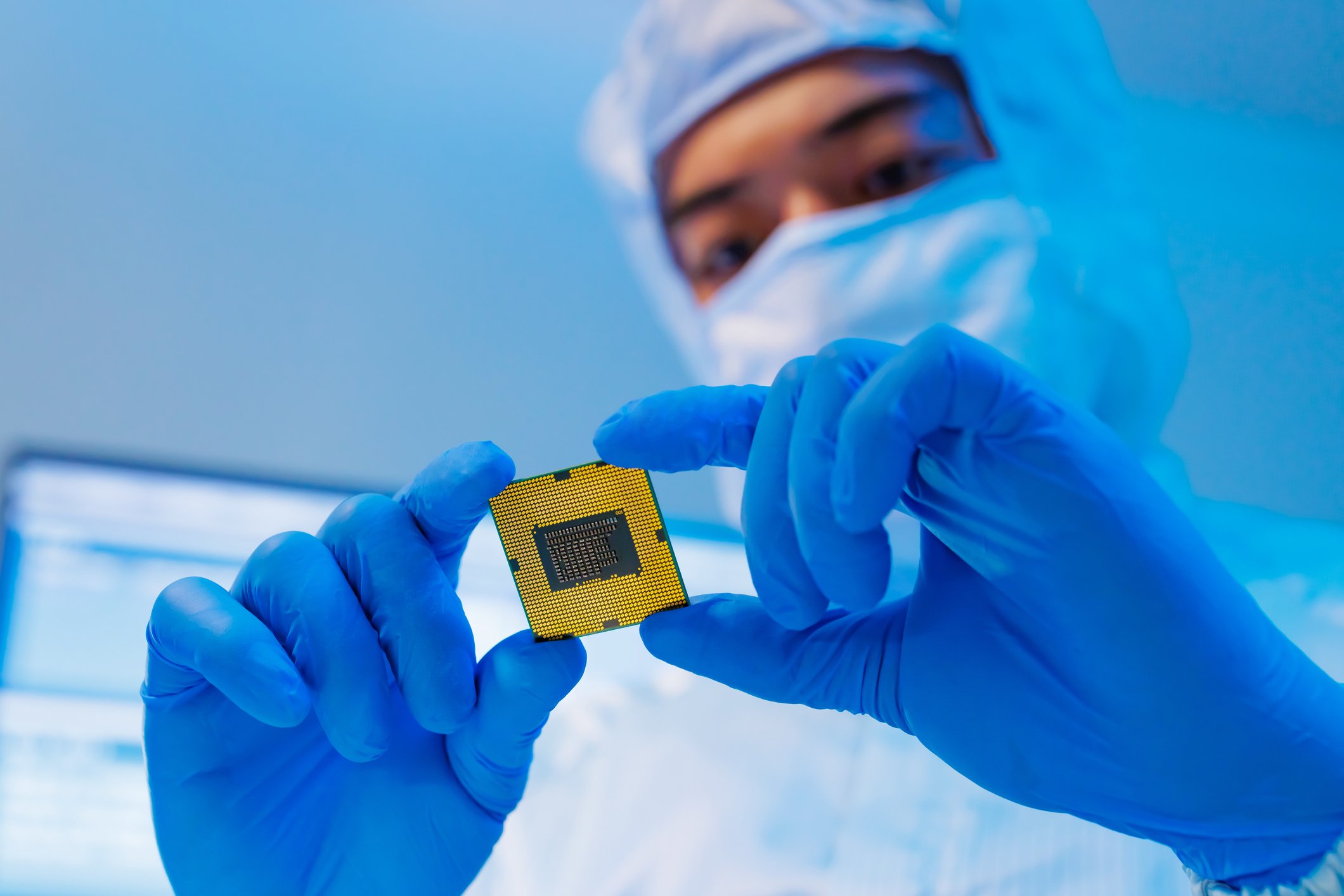
This is an essential process in various fields such as semiconductors, optical devices, solar cells, and sensors.
Thin film deposition techniques are broadly classified into "Physical Vapor Deposition (PVD)" and "Chemical Vapor Deposition (CVD)". In PVD method, the material is physically evaporated/dispersed and deposited on the substrate, whereas in CVD method, the film is formed using a chemical reaction.
Canon Anelva mainly handles the products that use sputtering, a method within Physical Vapor Deposition.
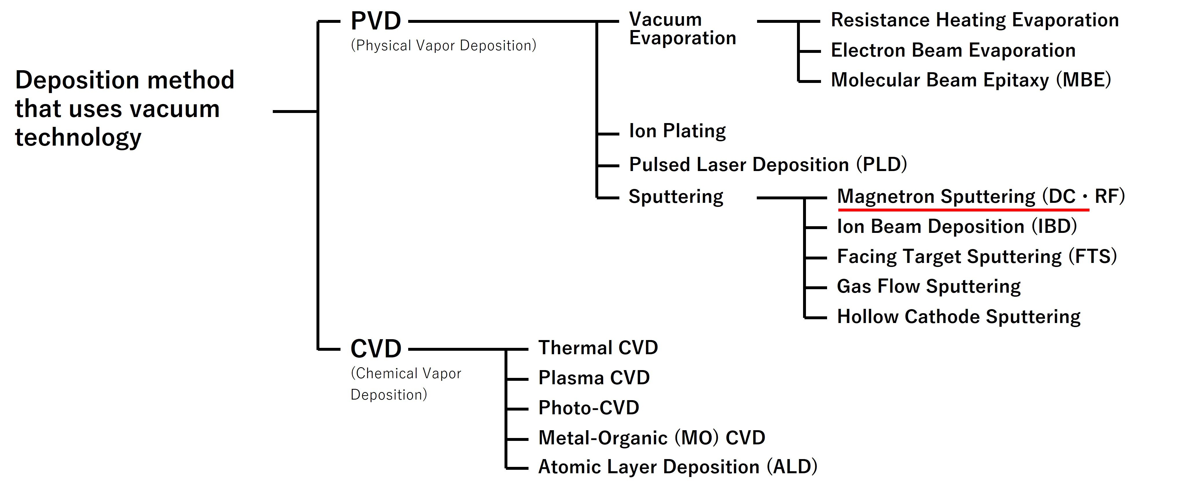
About Sputtering
"Sputtering" is one of the typical thin-film deposition methods in PVD and is mainly used to deposit materials such as metals and oxides as thin films on a substrate.
This technique is based on a physical process in which plasma is used in vacuum to eject atoms from the material surface and deposit them onto the substrate.
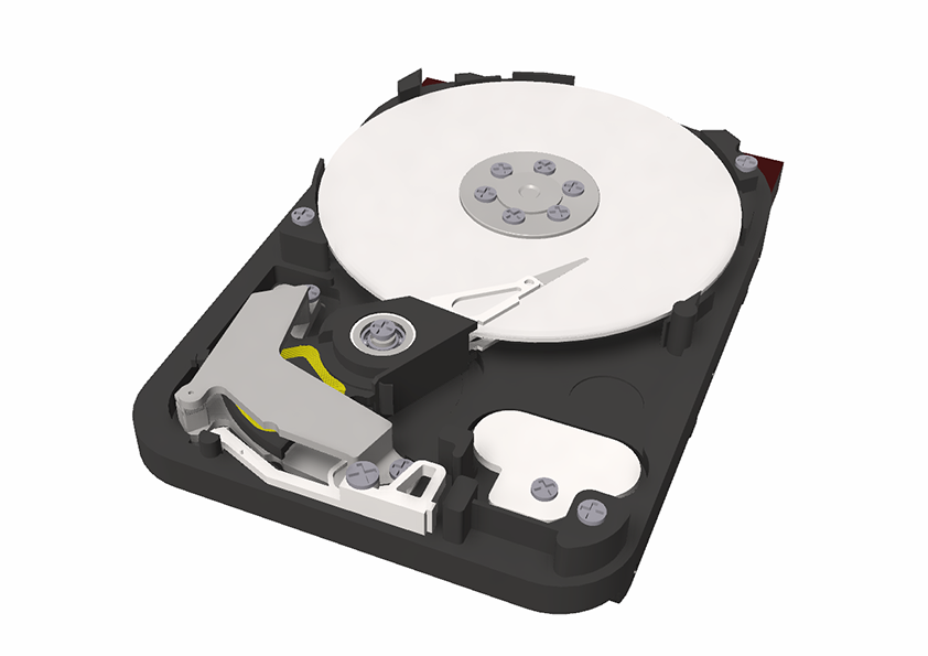
It offers excellent uniformity in film thickness, adhesion, and material versatility, and is widely used in fields that require precise thin-film formation, such as semiconductor devices, optical components, and magnetic storage media.
Sputtering is characterized by its ability to form denser and more controllable films compared to other PVD techniques such as evaporation.
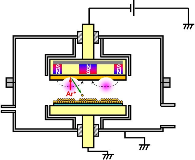
Principle of Sputtering
Thin-film deposition is mainly carried out based on the following principles.
1.Place the target (deposition material) and the substrate inside a vacuum chamber.
The target is the material to be deposited as a film, and the substrate is the surface on which the film will be deposited.
2.Introduce an inert gas such as argon into the chamber and generate plasma.
By applying a high voltage, the gas becomes ionized and enters a plasma state.
3.Ions in the plasma collide with the target, causing atoms to be ejected (sputtering).
This collision causes atoms and molecules to be released from the target surface.
4.The ejected particles accumulate on the substrate, forming a thin film.
This accumulation results in a uniform, high-quality film.
Canon ANELVA provides the manufacturing equipment utilizing sputtering techniques.